In the CBN Clean Room laboratory (approx. 100 sqm, class 1000/10000), the complete front-end technologies for microfabrication of semiconductor and polymeric -based passive and active piezoelectric Micro-Electro-Mechanical-Systems (MEMS) for energy harvesting and biosensing are installed. Parallel and serial nanofabrication techniques are also settled and can be pursued for photonic and plasmonic bio-sensors. The Clean Room includes micro/nanopatterning tools (Mask Aligner, 3D Lithography system, Imprinting Lithography), deep dry etching tools (ICP Oxford Estrelas100, STS ) and tools for devices inspection and characterization (Optical Microscope and Profilometer). Access to the instruments is limited to trained people only.
The person in charge for the lab is Dr. Tiziana Stomeo
Mask Aligner SUSS MA8/BA8
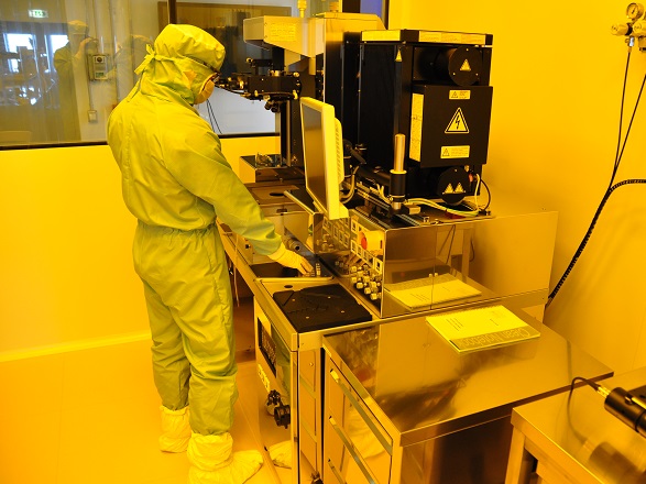
Süss MicroTec MA8/BA8 is standard UV litography tool for exposing through mask. Designed for operator-assisted alignment and exposure of wafers up to 150mm and square substrates and is suitable for industrial research and production of micro-devices, optical devices and MEMS. Exposure can be carried out in proximity mode or in contact mode. Vacuum contact offers highest resolution of pattern transfer, but also highest mask wear. MA8 is equipped with top side optical microscopes and bottom side microscopes, so alignment is possible from both sides of the wafer.
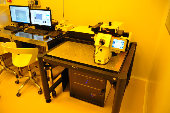
Nanoscribe Two photon Lithography
Nanoscribe’s Photonic Professional is a table-top laser lithography system capable of true three dimensional micro- and nanofabrication of photoresists. The core ability to create almost arbitrary complex 3D structures is enabled by a nonlinear optical phenomenon called 2-photon polymerization. This allows to directly write 3D micro- and nanostructures into photosensitive materials, e.g. SU-8, Ormocere, AZ- or IP-photoresists with different chemical and/or physical properties.
Spray Coater EVG
The EVG spray coater allows pieces up to 8" wafers to be spray coated with photoresists and potentially other types of polymers or atomizable materials. Spray coating is necessary when a uniform coating is required on a highly topographic surface. Resist is loaded in a syringe and dispensed using a step motor. Spray nozzle programmable parameters: Speed (rpm), acceleration (rpm/s), absolute position.
Dektak XT Profilometer
The Dektak XT is a thin film step height measurement tool capable of measuring steps of ~ 500Å to 150um. The Dektak XT also has thin film stress analysis software and 3D mapping capabilities. The technological breakthroughs incorporated in Dektak enable critical nanometer- level surface measurements for the microelectronics, semiconductor, solar, high-brightness LED, medical, and materials science industries.
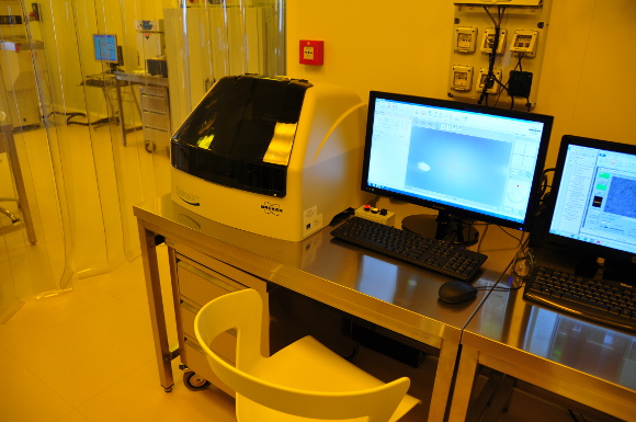
Nikon Eclipse L200NSD Microscope
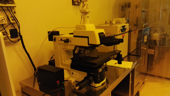
For routine laboratory use for biology and industry, the Nikon Eclipse L200NSD Microscope provide a high quality, compact and easy-to-use polarizing microscope, enabling more advanced polarizing microscopy.
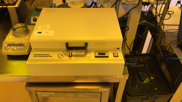
Bromografo Bromograph
The bromograph is used to transfer pattern on a photosensitive resist in case of a micrometric precision is not needed. A bromograph (or UV Exposure Unit, or UV Screen Exposure System) is a fundamental instrument for making PCBs using the photo-etching method without using a Mask Aligner.
Hydrofluoridric Acid Vapor Phase Etcher
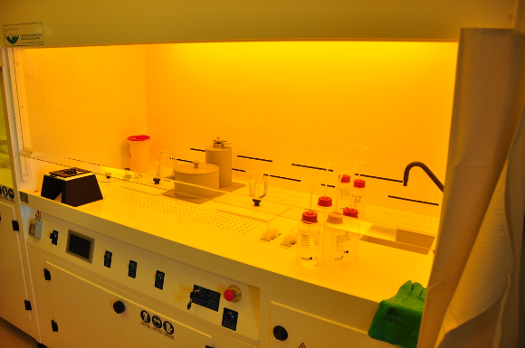
Hydrofluoric acid (HF) vapor allows fast etch rates and is highly selective etching of silicon oxide against silicon. A typical application for HF etching is the removal of sacrificial oxide layers in MEMS fabrication by working entirely in the vapor phase without sticking.
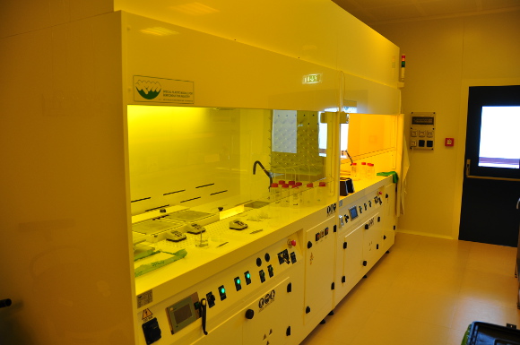
Solvent and Acid chemical Hoods
Two hoods allow to distinguish clean room operations for wet-etching based microfabrication and lithography based chemical development, respectively.
Spin Coater SUSS
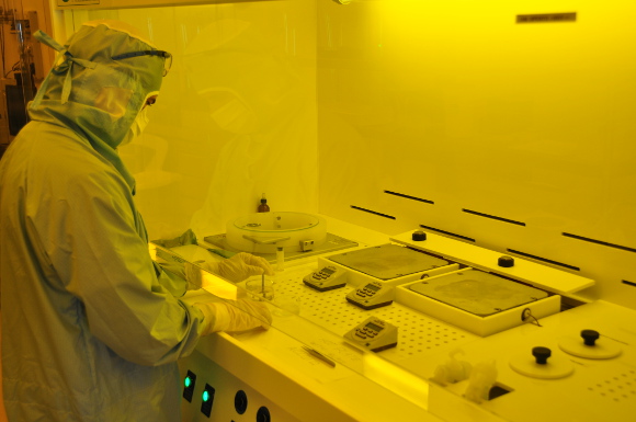
This equipment is used to deposit thin layers of photoresist onto flat substrates by spinning the substrate and allowing the centrifugal force to evenly distribute the photoresist. Spin Coater SUSS represents the next generation of manual spin coater and developer systems that have been developed specifically for laboratory and R&D. Designed for a variety of photolithography chemicals, Spinner systems provide uniform, precise and repeatable spin coating results on the wafer through its advanced cup design.
Critical Point Dryer
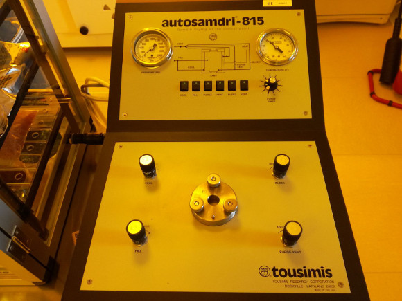
For drying wet-etched 3D complex samples without suffering sticking on the substrate. Primarily used for the processing of lifesciences and geological specimens, the Critical Point Dryer will be used for the controlled drying MEMs and aerogels.
ICP Oxford Estrelas and STS ICP
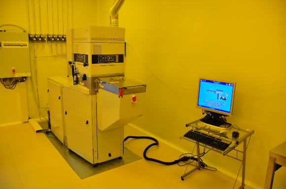
inductively coupled plasma -based etchers for Deep Etching in Silicon substrates (Bosch process) and III-V based semiconductors. The combination of high density ICP power, and low pressures can result in very high etch rates, with an anisotropic profile. By varying the ICP source RF power, and bias RF power the ion energy or ion density can be controlled that allows for a large process window.
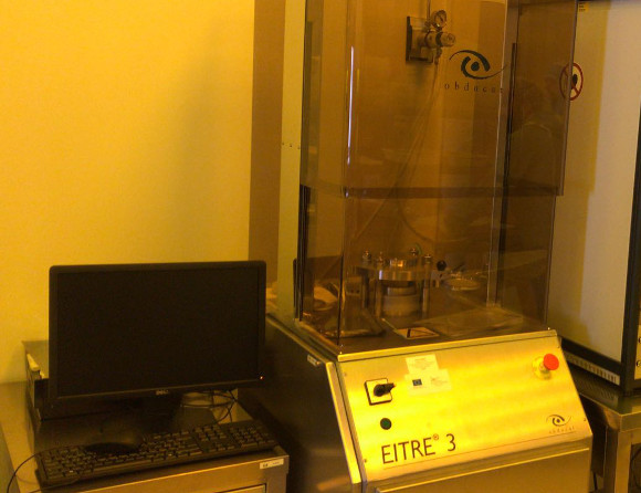
Obducat Eitre3 NanoImprinter
Thermal Imprinter Obducat Eitre 3 performs Nano Imprint Lithography (NIL) by replicating a desired pattern from a master to a target substrate (up to 3 inches) using a resist film. The resist can be the actual target substrate or it is deposited on a substrate material, which is then etched for the pattern transfer.
Oxygen Plasma Asher
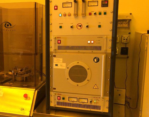
for cleaning of organic layers on substrates and oxygen-based treatment of surfaces. Through Plasma ashing, organic and polymeric residues are removed from the surface without removing any other part of the surface leaving behind just the desired pattern on the surface of the material. It is also used for hydrophilization of surfaces.